Practical control delay self-extinguishing switch circuit diagram
Circuit
The following figure shows the electrical schematic diagram, sound, light, touch control delay self-extinguishing switch the circuit from the power supply circuit, the signal detection conversion circuit of the delay circuit and control circuit.
1 circuit
(1) the power circuit. The circuit consists of diode Dl, D2,, and D3, and D4, resistor Rl, R2 and capacitor Cl. D1 ~ D4 form a bridge rectifier circuit, its function is the load (light bulb), 220V AC adapter for DC, the high DC voltage, Rl, R2, and Cl on the rectified pulsating DC voltage step-down and filtering . Cl at both ends of the voltage is the follow-up unit circuit supply voltage is about 9.5V.
(2) signal conversion circuit is detected. The circuit contains a light, conversion of voice and human touch signal detection. Light detected by the R5 and photoresistor RC, the voltage across the photoresistor varies with the intensity of light changes, and into the IC CD4071, 1,2 feet for processing; sound detection by the electret microphone MIC C3, R4, R5, R6 and Ql the composition of the sound signal by the MIC converted to electrical signals through the capacitor C3 coupled to the transistor Ql amplification, and resistors R4, R5 constitute the Ql DC bias resistor, sound or absence of Ql collector voltage changes to the IC CD4071 1,2 feet for processing, the resistor R6 provides bias for MIC internal amplification components; human touch sensing signal through the touch tablet, R3, and C3 into Ql amplification from Ql C 1,2 feet voltage change input to the CD4071 1,2 feet, whether the touch signal will cause the CD4071, CD4071 1,2 feet voltage is the result of joint action by the sound and touch signals.
(3) delay circuit. The circuit consists of D5, R7 and C2. R7 and C2 is the delay time control device, shown in the figure parameters of delay time is about 150s. The function of the diodes D5 is the prevent C2 CD4071 4-foot discharge impact delay time.
(4) control circuit. The circuit consists of IC CD4071, one-way silicon controlled rectifier SCR1 and R8. The CD4071 is four hundred and twelve input OR gate.
 You are here: News
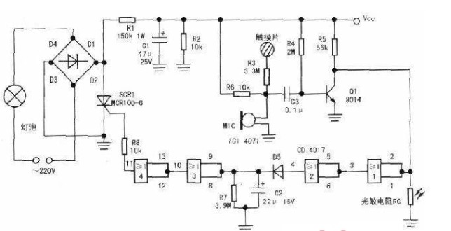


 BOM component procurement