Click >>>
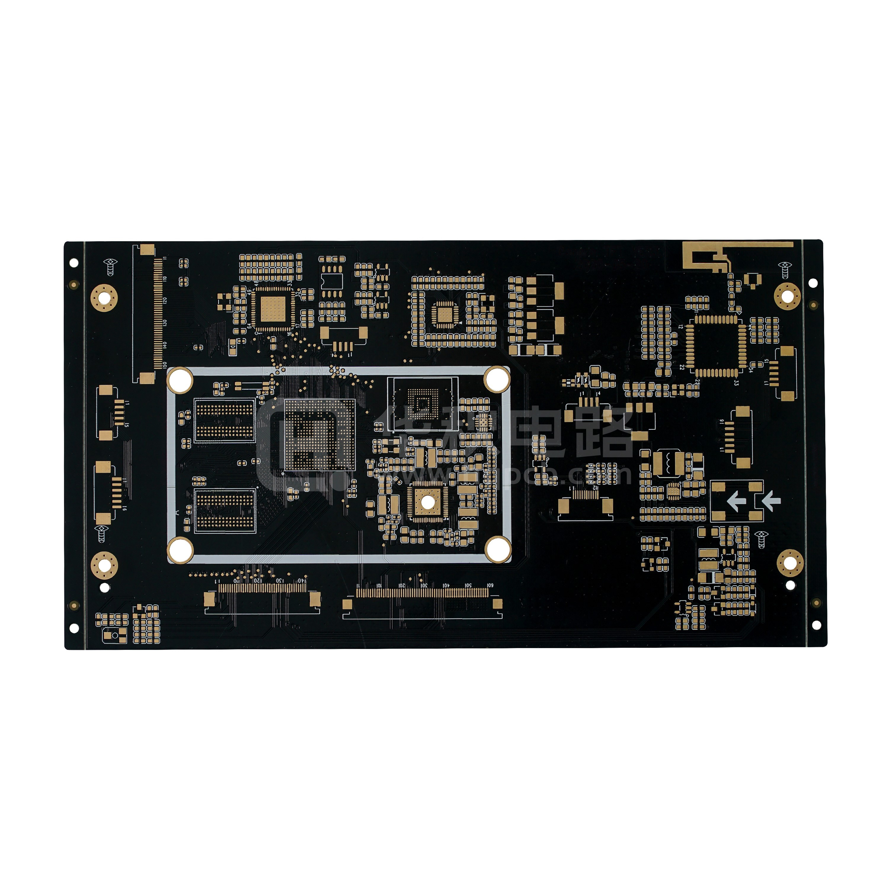
1.PCB includes MCPCB, R-F PCB, HIGH Multi-Layer, High-Density Layer, HDI Layer, Lmpedance Control Layer,
High Tg Layer, Thick Copper Layer And Other High-End Circuit Layers.
2.The max. layers: 1~48 layers
3.The largest dimensions: 864 x 610 mm (34" x 24")
4.The most thickness: 315mil(8mm)
5.The smallest route spacing: 3mil/3mil
6.The smallest finished hole: 6mil(0.15mm)
7.The largest aspect ratio: 12:01:00
8.Impedance control: ±5%
9.Surface arts and crafts: Aluminum(No Aluminum), spray tin, gold, silver, tin, gold finger, hard gold, antioxidant
10.The original materials: FR4,Tg:130℃-170℃,Rogers, Arlon,Taconic
11.Special arts and crafts: Blind & buried hole, through hole, a hole, a countersunk hole,after the hole,
crimping hole, gold finger PCB, metal substrate PCB
Sample Lead Time:
5 days : Single Sided and 2 Layer
7-14 : Multi-Layer
Production Lead Time:
7 - 14 days : Single Sided and 2 Layer
10 - 20 days : Multi-Layer
Express lead time:
Double sided :24 hours
4 layers :48 hours
6 layers :60 hours
8 layers :72 hours
10 layers : 96 hours
10 layers above :96 hours


 BOM component procurement
 You are here: